5G kommunikationskort PCB design case
[Enkeltplade type] 5G RF kommunikationstavle (VPX arkitektur)
[Pin-nummer] 10731
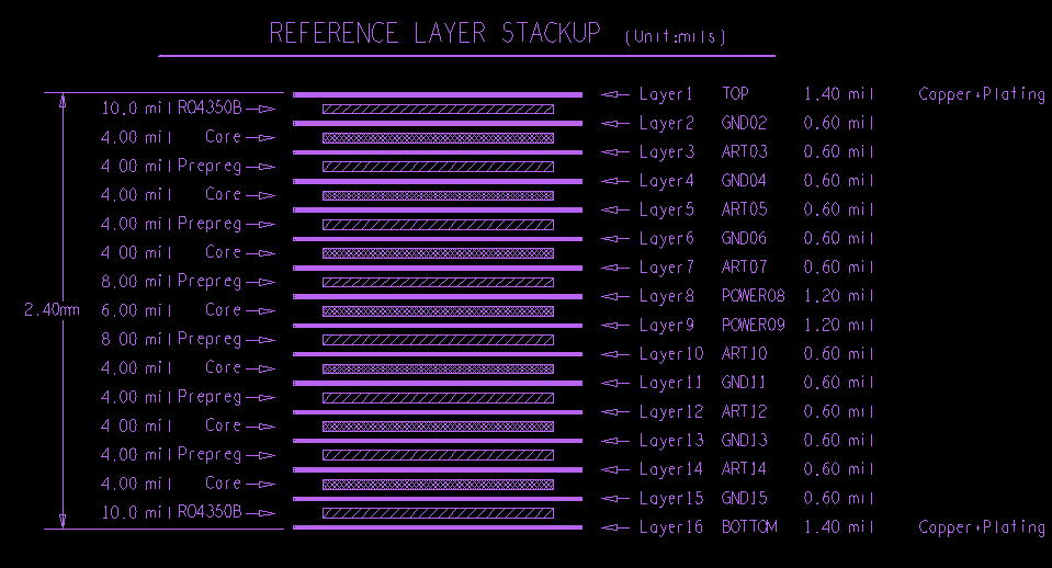
[lag] 16 lag
[Maksimal sats] 10Gb/s
[Vanskeligheder]:
1, Der er 8 RF kanaler, RF-linjehastigheden er 2,5G, og kravet til signalintegriteten er højt;
2, Pladens tykkelse er 1,6 mm, og antallet af laminater er begrænset;
3, RF-delen er mere, skal lave varmeafledning og afskærmning;
[Vores modforanstaltninger]:
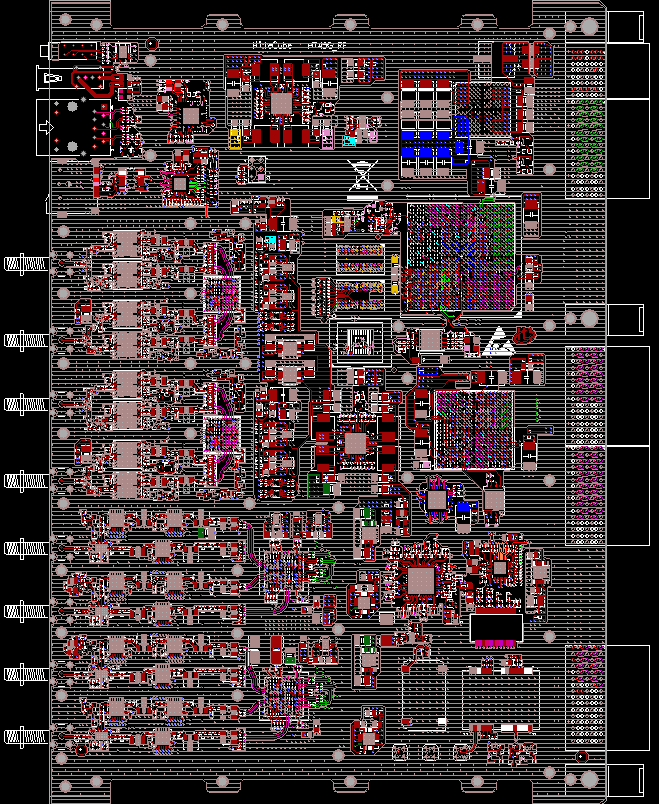
1.Ifølge VPX-arkitekturen, kunden kræver der er 8 RF-grænseflader, indikatorlys, USB, netværksport og TF-kort. Panellayoutet er stramt. Gennem evaluering, det er nødvendigt at overveje layoutet for at komprimere bredden af layoutet over Y-aksen af RF-kredsløb. afskærmningshulrummet på 2 mm bredde tilføjes til hver RF, og skjoldhulrummet i den fulde version er reserveret; layoutet er som følger:
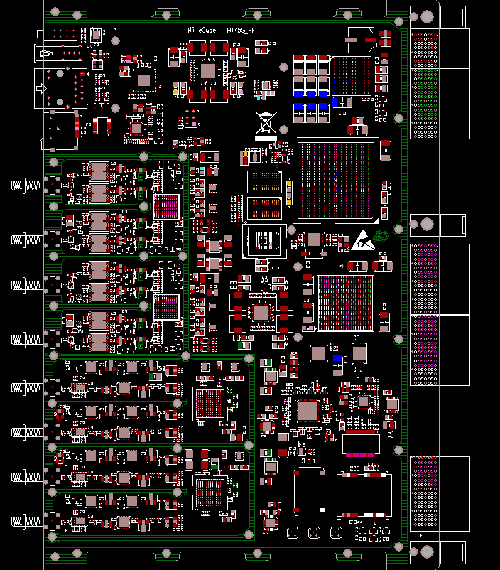

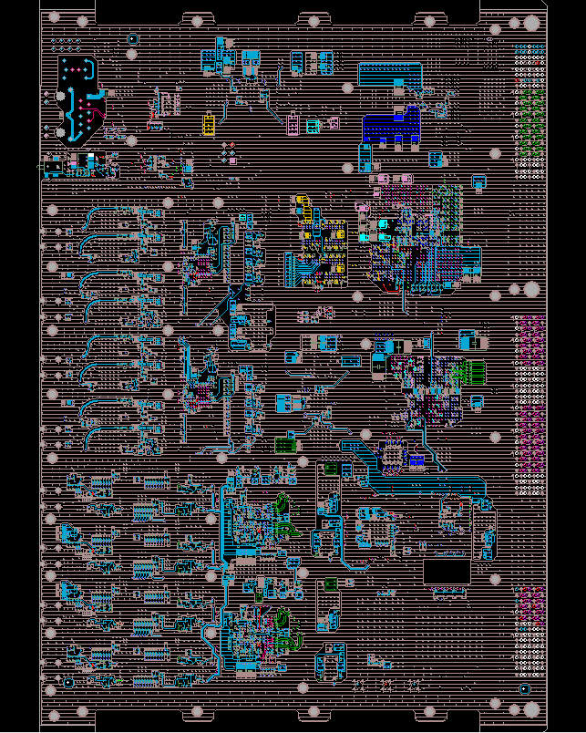
2.På grund af at overveje pålideligheden af RF-signalet, 1-2, 15-16 direkte brugt RO4350B, tykkelsen er 10 mil, RF-spor behandles i det øverste eller nederste lag, ingen behov for reference isolering
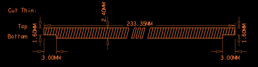
3.Bestyrelsen nær det øverste-nederste lag ved hjælp af RO4350B, tykkelse er 10MIL, hvis håndtere det som 1.6MM , der vil kun være 1,1 mm tykkelse til at stable den digitale del,det kan ikke opfylde kravene i rute.efter at have kommunikeret med kunder og givet råd, ved hjælp af stigeprocessen,behandling som 16-lags , det øverste lag behandler kun RF-kredsløbet, og de digitale delspor er alle arrangeret behandling i det indre lag , og det øverste og nederste lag skal vandes GND kobber for at sprede varme og skærme.
4.På grund af den høje varme, der genereres af RF-kortet , ud over RF-signalet, de resterende tomme områder af det øverste-nederste lag behandles som kunstvanding GND kobber, og øge varmebehandlingen.